Research Interests
Nanoscience - Nanocrystals.
Preparation, Fabrication, Characterisation, Application.
Nanocrystals Synthesis and Functionalisaion
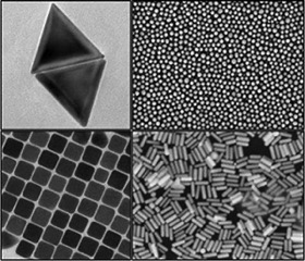 Nanocrystals are normally known as those very small particles constructed by hundreds or thousands of atoms
with dimensions range from 1-100 nanometres. They exhibit unusual, size-dependent optical, luminescent, magnetic
and electronic properties. Nanocrystals can be wildly used in many areas of aspects, such as colour displays,
drug delivery, solar cells, fast bio-sensing, etc. Those amazing properties highly dependent on nanocrystals for their
kinds (eg. gold, silver, silica, etc), size (monodispersity, nanometer-scale), shape (triangle, sphere, cube, rod, etc.),
surface properties (coating, ligands, etc.), and so on.
To fully realise those outstanding properties in practical applications, one of the biggest research areas
is to develop the methods to synthesis nanocrystals in solution with controlled morphology,
high monodispersity, and designed surface functionalisation.
Highly controlled and efficient synthesis methods can guarantee the further study of other properites of nanocrystals.
I am interested in studying synthesis methods of gold, silver, platinum, palladium nanocrystals and other inorganic, semi-conductor nanocrystals.
(Figure: Gold nanocrystals
with different shapes. Copy right reserved.)
Direct Assemlby and Nanofabrication
 One of the biggest challenge in modern nanoscience and nanotechnology is how to effectively convert chemically
synthesised nanocrystals into a solid-state device for general applications.
In other words, in order to apply the excellent properties of nanocrystals to real life applications,
it is inevitable that the nanocrystals synthesised in solution will need to be efficiently prepared into devices that can be used in practice.
Most of the nanocrystals are produced in solution for better morphology control and large scalability.
However, it is not feasible to take a vial of liquid using in common.
Although, nanocrystals can be easily coated onto the substrate by drop casting or spinning coating.
It somehow screened most of the nanocrystals properties due to aggreation and disorder on the surface.
A highly effective method to assemble nanocrystals from solution onto a substrate with controlled order and pattern
can maximumly realise the potentials of the assembled nanocrystals.
The direct assembly method is the approch that directly assemble synthesised nanocrystals on a
pre-pattern substrate to fabricate designed structure without chengeing their intrinsic properites.
The key factor for a successful direct assembly is to apply a proper external driving force to push or drag the nanocrystals
onto the designed locations on the substrate.
My current research focus is developing direct assembly method for single nanocrystal arrays by Electrophoretic Depsition.
(Figure: Adapted from 10.1002/adma.201904551. Copy right reserved.)
Nanocrystals Optical and Electrical Properties
 The size-dependent optical and electrical properties of nanocrystals attract great attentation a long the hunman history.
For example, stained glass, wildly used in churches, is credited to the mixing of glass and metallic nanoparticles.
It makes the glass vibrantly coloured but still retain its transparency.
The latest QLED TVs are now also based on extensive scientific research,
evolving from the electrofluorescent properties of quantum dot nanocrystals.
Due to the ability of quantum dots to emit highly homogeneous, monochromatic light under the excitation of electrons,
the colours presented by OLED TVs are more vibrant and have a higher contrast ratio.
At the current time, many studies regarding the "colour" of nanocrystals have been carried for better understanding.
And researchers are already able to tune the optical and electrical properties by selectively synthesis nanocrystals with a given morphology.
The optical and electrical properties of nanocrystal have been wildly used in many area of aspects such as, security features,
coloured displays (eg. QLED), biological labeling and sensing, etc.
A deeper research and understanding of optical and electrical properties of nanocrystals can promote their pracitcal application.
(Figure: CdSe based Quantum Dots. Copy right reserved.)
Single Particle Spectroscopy
 As well known, the outstanding properties of nanocrystals are highly dependented to their size and shape.
One of the big challenge in nanocrystals research is how to study the relation between morphology of the nanocrystals and
their properties.
For example, the quantum size and fluorescence properties of cadmium selenide quantum dot (CdSe) nanocrystals are highly correlated with their size.
A size difference of 3-5 nm can lead to a fluorescence colour of CdSe quantum dots ranging from none to red to purple.
One inevitable fact is that it is nearly impossible to control all nanocrystals with absolutely identical morphology
with current synthesis technique. Therefroe, the results of common characterisation can only represent the ensemble property of all
nanocrystal with minor differece. In order to have a more sophisticated understanding, it is necessary to isolate the
distraction and only study one selected nanocrystal to link its unique morphology and property. It terms of optical properties, I use
advanced optical microscopy, such as dark field microscopy, wild field microscopy, confocal microscopy etc., to study single nanocrystal.
(Figure: Nikon Dark Field Microscope. Copy right reserved.)
Numercial Modeling and Simulation
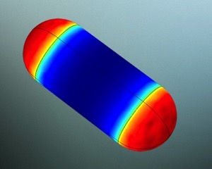 The numercial modelling and simulation is one very powerful tool to study the properties of nanocrystals.
Theorical simulation and practical experiment can support each other during reserach.
On one hand, with known facts of practical experiment, we can compare results with numercial model to support the
reliability of the simulation. On the other hand, by tunning the parameters in numercial model, the simulation results
can be used to predict and guide our practical experiment. In addition, in combine with the classic theory, the
numercial simulation can be used to support and explan phenomenon performed from nanocrystals or nanocrystal based devices.
COMSOL Multiphysics is the simulation software that I mainly used.
By selecting physics module that corresponds to the actual experiment, creating an experimental model that matches or approximates the actual
experimental conditions, setting the physical parameters, dimensions and other conditions to the object of study,
and specifying the physical field boundary conditions, COMSOL simulations are able to restore or predict
the specific physical behaviour of the object of study under the set conditions to the greatest extent possible.
Key Physics: Optics, AC/DC, Heat Transfer and Structural Mechanics.
(Figure: Electric field distribution on gold nanorod under light illumination. Copy right reserved.)
Nanocrystals Device and Application
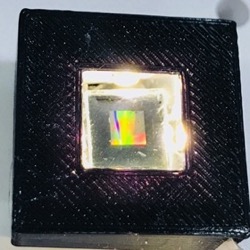 The thrive of technoloy is supported by the growth of science, and science is flourishing credited to realisation of the technology it supports.
It is also very important in nanoscience to convert those excellcent properities of nanocrystals into devices for practical applicaiton in common.
Based on the inherent properties of the different nanocrystals, nanocrystals have the potential to demonstrate their unique appeal in all aspects of social development.
For the nanoscience I am interested in, I devote to explore the possibilities to transfer the fundmental research into a prototype device or proof
of concepts for certain application. For example, by sophistically designing the structure, a pattern that constructed by arrays of gold or sliver
nanocrystals can be adapted for advnaced security features for anti-counterfeiting. The An array of dense fluorescent quantum dots can be used
to develop the high resolution and high fidelity colour displays. (Figure: Array of gold nanorod illuminated by LED and exhibit rainbow colours.)